Excessive power consumption is a major risk in digital design as it may lead to timing failures and inconsistencies, overheating issues, and performance degradation, which can be specifically problematic for energy-efficient and battery-powered systems. While SAIF-based power analysis can accurately predict the average power consumption in a design by analyzing changes in signals over time, it does not indicate the exact timing of signal transitions. In such scenarios, using waveform traces proves the most effective as it allows tracking signal transitions at each timestamp within each clock cycle and quickly detecting when any irregular power spikes occur.
To facilitate faster and more efficient chip power profile estimation in digital designs, Antmicro has implemented new power analysis workflows that allow detecting excessive power consumption based on VCD trace outputs: peak power analysis that shows when a simulated design consumes the most power, glitch power analysis that determines how much power is attributed to unwanted transitions caused by bugs in the design logic, and scoped power analysis that generates a power consumption report from a single user-specified module.
Originally implemented for a customer project, these workflows are built around the OpenROAD toolchain alongside other open source solutions - the popular Verilog simulator Verilator, Antmicro’s open source tool for fast VCD data preprocessing trace2power, and the static analysis library used by OpenROAD - OpenSTA.
In this blog note, we describe our implementation of the peak, glitch, and scoped power analysis workflows using Verilator, trace2power, and OpenSTA, and showcase how to run these workflows to quickly identify and optimize power-inefficient parts of ASIC designs.

Power estimation in digital designs with OpenROAD
As an active contributor and official member of the OpenROAD Initiative, Antmicro has been designing, customizing, and optimizing digital chip designs that leverage the OpenROAD toolchain for years. Such developments also stem from customer projects and revolve around open source tools as evident from our implementation of a genetic algorithm for improved design resynthesis, extended technology mapping for design optimization, and automatic clock gating for lowering power consumption.
In order to run any of the introduced OpenROAD-based power analysis workflows for your digital design, you first need to have it processed with synthesis and place and route steps using the OpenROAD-flow-scripts as described in the Prerequisites section of the Power analysis workflows repository.
Estimating peak power consumption
The peak power estimation workflow makes it possible to determine at which particular point in time the design is consuming the most power. This is achieved through the separation of signal transitions by clock cycles with trace2power, which reads and extracts the accumulated power activity data so that each cycle can be further processed individually with OpenSTA.
The peak power estimation workflow involves the following steps:
Generating VCD files. This step uses the synthesized design to run simulation in Verilator and produce a VCD file containing every signal transition that happened during the simulation.
Processing VCD files with trace2power. At this point, two Tcl files are generated: a Tcl script used to calculate base power usage (i.e. power consumption without any signal transitions) and a separate Tcl script generated for each clock cycle used to calculate power consumption per clock cycle.
Generating a peak power report. This last step involves running the peak power Python script which feeds each Tcl script to OpenSTA to calculate power consumption per clock cycle.
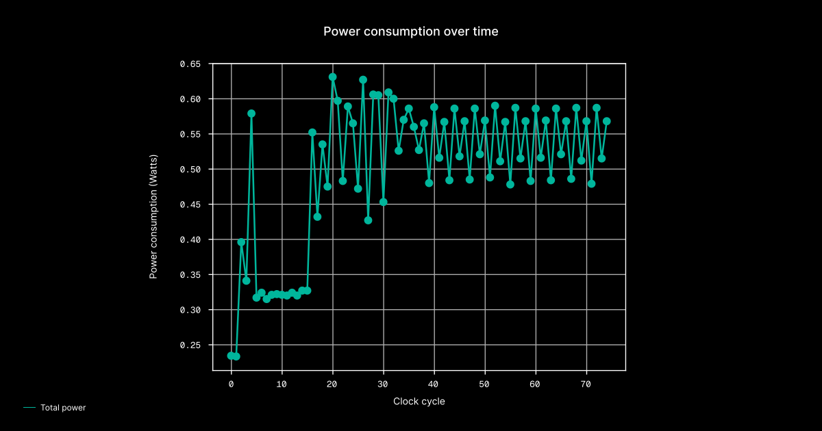
The Python script produces a plot with power consumption data per clock cycle over time where the highest points indicate peak consumption, as illustrated in the example below:
For detailed instructions about generating, processing, and analyzing peak performance data, refer to the relevant section in the README.
Estimating glitch power consumption
Glitches are transient changes in a circuit state that occur during a clock cycle as the state stabilizes. While being an inherent aspect of any digital design, glitches can significantly affect its power consumption.
By running the glitch power estimation workflow, you can identify how much power is consumed by these unwanted transitions, which is achieved through analyzing signal transitions in each clock cycle and dumping only those that change more than once. The output with all such transitions is passed to OpenSTA, where the power estimation is performed only on those glitches.
Glitch power estimation involves steps similar to the peak power estimation workflow:
Processing VCD files. The main difference from the previous process is in the way Tcl scripts are generated: instead of storing each signal transition per clock cycle, trace2power stores only those where the signal changed its value more than once.
Generating a glitch power report. Tcl scripts for glitch power consumption are fed exactly the same way as peak power consumption scripts and can be plotted on a graph showing power consumption over time, as demonstrated on the following plot:
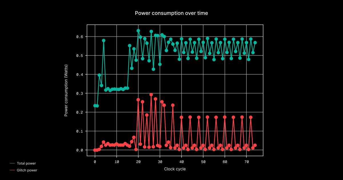
In this example, the red graph represents the glitch power consumed during the stabilization process. For detailed instructions about generating, processing, and analyzing glitch performance data, see the aforementioned README.
Conducting scoped power estimation
The scoped power estimation workflow is applicable in scenarios where it’s necessary to identify which parts of the circuit are using excessive power, being particularly important in large and complex digital designs.
The power estimation is made on a module-by-module basis, which requires the design to be first synthesized with its hierarchy preserved. After that, you can separately calculate power consumption for each building block by limiting the exact design scope with the help of the --limit-scope-power command-line option in trace2power. This command will generate a scoped power consumption report having the same format as the static power analysis report, which we covered in detail in an earlier blog.
You can find detailed instructions on how to perform scoped power estimation in the same README. For information about the supported commands and arguments in trace2power, read the libtrace2power documentation.
Design ASICs faster and more efficiently with Antmicro
The introduced peak, glitch, and scoped power analysis workflows help to significantly reduce the time needed to analyze power consumption in an electronic circuit design and provide developers with the exact temporal information about any detected power irregularities.
By building power estimation workflows based entirely on open source, specifically the OpenROAD toolchain, Antmicro helps to lower the barriers of cost, time, and vendor dependency in modern silicon development, which manifests in the growing variety of customer projects that leverage the benefits of our open source tooling.
If you are interested in adopting open flows for your ASIC designs, would like to create reusable ASIC and FPGA IP cores, including next-gen RISC-V-based ones, or accelerate your digital design development with our ASIC&FPGA developer productivity tools, get in touch via contact@antmicro.com.