The ASIC design and manufacturing flow has for a long time been dominated by proprietary tools and processes. The growing complexity of chip-building has been reinforcing the claim that “hardware is too hard to be open source”, as the cost and time needed to build an ASIC have kept small, more agile, software-oriented teams and individuals away from the hardware domain. Thus, ASICs have not been able to benefit from the enthusiasm and collaboration which have been fuelling software development for decades now. Thanks to the continued effort of many entities which Antmicro is very proud to be among, this is now changing quickly.
RISC-V: Openness-driven innovation
The first shift in the walled garden, proprietary chips design landscape came with the creation of the RISC-V Foundation in 2015 centered around the open source RISC-V ISA. Antmicro has been on board as a Platinum Founding Member of the Foundation (now, several hundred members strong, transitioning into a Swiss-based entity called RISC-V International) since the very beginning, as it reflected our belief that an open source approach can - and is bound to, eventually - revolutionize all areas of computing, even the less obvious ones.
RISC-V proved ASIC design can be a collaborative process, with players big and small working together to compliment each other’s strengths not only in developing the ISA but also many of the tools needed to make it practically useful. For example, Microsemi worked with SiFive to provide the SoC complex at the heart of their new and exciting PolarFire FPGA SoC, and then turned to Antmicro to provide a simulation environment - using our open source Renode Framework - to make development possible before the SoC hits the market later this year. The OpenTitan project, driven by key RISC-V adopters Google and Western Digital together with the UK not-for-profit lowRISC, strives to build a more transparent, trustworthy, high-quality reference design and integration guidelines for silicon Root of Trust chips. Such examples abound in the RISC-V world, but the un-core, design tools, verification and other parts of the ecosystem have mostly remained closed.
Enter CHIPS
Established in 2019, CHIPS Alliance takes the open, collaborative aspect of RISC-V even further. CHIPS wants to generate and integrate fully open source, high quality IP and tooling for ASIC design; the organization extends beyond cores and specifications, and acknowledges the importance not only of the result but the process itself; thus, the aim is to make both ASICs and the ASIC design processes open source all the way. Why? Again, a lesson learned from software: if you open up to collaboration, adaptation and change on all levels, the long-term results will be surprisingly good.
CHIPS has been home to such important projects as the Chisel HDL, the Rocket core generator and related tools, the SweRV cores or AIB interconnect. There is work under way to enable fully open source SystemVerilog/UVM support in tools like Verilator and Yosys (with some milestones like fully open source linting, formatting or synthesis of SystemVerilog code already accomplished), opening the door to more open source collaboration around design verification which constitutes the highest cost in modern chip design.
Also in the tools area, the very ambitious OpenROAD project, also a CHIPS member, is a DARPA-backed activity aiming to create a fully open source, quick, automated digital design flow. If you want to see how open source, automated chip design might look like in the future, see OpenROAD’s excellent ChipKit tutorial from ISCA 2020.
Aggregating those activities a vastly different landscape begins to emerge, one where chip design can be innovated upon on various levels, and teams can go back and forth between hardware and software optimizations for new use cases such as machine learning without NDAs and costly licences. But - until now - there was one element notably missing.
First ever open source PDK
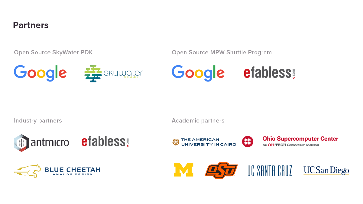
We are excited to announce Antmicro’s participation in yet another historic first in the area of semiconductor process technology. In a project led by Google and SkyWater Technology, and in collaboration with partners including Antmicro, Blue Cheetah, efabless and numerous Universities, an open source SkyWater PDK (Process Design Kit) for the 130 nm MOSFET fabrication process, along with related sources, is being made available. This development greatly lowers the cost of entry into chip manufacturing and paves the way for even more exciting collaborations to happen in the open source silicon domain.
For some background, a PDK is a set of data files and tools used to model a specific process in a given foundry used with EDA (Electronic Design Automation) tools in the chip design flow. PDKs traditionally have been closed - to the point where some would say it’s impossible to make them open! This collaboration, where Antmicro worked together with Google and efabless to convert the PDK data for the public release, is an important step towards truly open source chips. The 130nm PDK process is a mature technology that is useful for a range of applications, especially in the area of microcontroller development and research as well as mixed signal embedded designs and other use cases which combine digital and analog circuits. The SKY130 technology stack consists of:
- 1 level of local interconnect
- 5 levels of metal
- Inductor-capable
- High sheet rho poly resistor
- Optional MiM capacitors
- Includes SONOS shrunken cell
- Supports 10V regulated supply
- HV extended-drain NMOS and PMOS
SkyWater is an American technology foundry accredited by the US Department of Defense, which offers custom integrated circuit design and manufacturing services. It is predicted that the launch of the open source SKY130 process node will be followed by other, more advanced nodes, ultimately enabling more advanced processor applications, including ones that are Linux-capable.
The inaugural talk by Tim Ansell
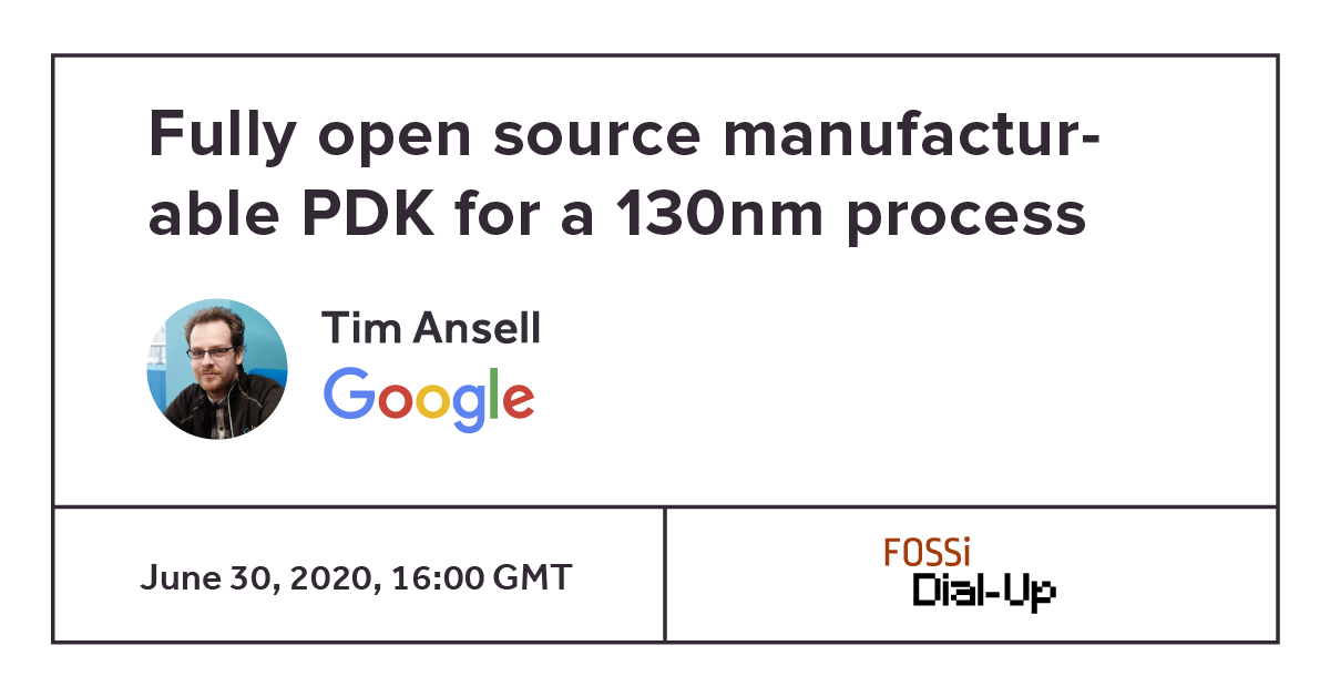
On Tuesday, June 30 at 16:00 GMT, Google’s Tim Ansell will give a talk at the FOSSi Dial-up meeting, presenting a thorough overview of the technical details of the PDK, as well as outlining the project’s goals and its roadmap. The event will be livestreamed on YouTube and will be followed by a Q&A session, so tune in to find out more about this historic step towards an open, accessible and collaborative chip-making process.


