The open source DDR controller framework developed by Antmicro in collaboration with Google has been successfully used to demonstrate new types of Rowhammer attacks and develop new mitigation techniques. To enable memory testing of DDR5, the most recent memory standard deployed in data centers, some time ago we introduced the open hardware Data Center RDIMM DDR5 Tester. Since then, we’ve been working on adding DDR5 support to the Rowhammer testing framework and in this note we’ll describe these efforts, which resulted in a DDR5 controller that works with RDIMM modules and enables DDR5 memory vulnerability research.

Open hardware Data Center RDIMM DDR5 Tester
Our initial DDR5 work utilized the LPDDR4 test board that allowed experimenting with a single DDR5 IC using the DDR5 testbed. Now, thanks to the open source Data Center RDIMM DDR5 Tester, we are able to test whole DDR5 RDIMMs (Registered Dual In-Line Memory Modules).
The DDR5 tester contains an AMD-Xilinx Kintex-7 series FPGA in a 676-BGA package and exposes a single USB 2.0 interface that provides access to a 4-channel FTDI transceiver that allows reconfiguration of the FPGA and access to the debug console. A comprehensive overview of the board and its components is available on Antmicro’s Open Hardware Portal, along with a PCB stackup view and interactive schematics browser. The board was also described in detail in a previous blog note.
Since that note was published, the main effort of the project focused on preparing an FPGA design that enables support for DDR5 chips memory testing, including performing Rowhammer attacks.
Initial support for DDR5 memories
Adding support for DDR5 to the DRAM testing framework consisted of several steps. First, we worked on a DDR5 testbed with unregistered memory (a single DDR5 chip) to test the new DDR5 PHY. The training procedure, compliant with JEDEC’s JESD79-5A specification, starts with keeping the DRAM in a reset state until the clock stabilizes. The initial configuration, for which only MPC (multi-purpose commands) are allowed, involves Vrefs setup, bus termination and calibrating internal termination (ZQ). At this stage CA (command-address) and CS (chip select) lines aren’t trained, so their alignment to the DRAM clock is unknown.
Next, we enter CS training mode and find the best CS-to-CK (chip select to clock) alignment. Feedback to the training is provided by DRAM on the DQ lines. DRAM samples the CS signal on a positive clock edge and consecutive samples are split into batches of 4. Each batch is compared with the ‘0101’ pattern and when there’s a match, the DQ lines are set to low, otherwise they remain high.
Then we enter the CA training mode. This training stage searches for the best CA-to-CK (command-address to clock) alignment. The result is put on DQ lines as in CS training, but since CA is 14 bits wide, an XOR operation is used to reduce the bus to a single value. This value is then emitted on the DQ lines.
Once the CS/CA training finishes, the DRAM initialization can be completed using the more complex MRW (mode register write) commands. Before we enter the read/write training, we first have to set up PDA (Per DRAM Addressability). DRAM devices that share a single rank also share CA and CS buses. Without PDA, performing read and write training would be impossible, as data lines (DQ/DQS) aren’t equally long, so each DRAM in a rank requires a slightly different setup.
With all previous stages completed, we can start the read training. DDR5’s predecessor, DDR4, has a special register that stores the training pattern. DDR5 extends this feature, as it provides two 8-bit registers, an inversion register, a select register and 2 linear feedback shift registers (LFSRs). Read training can be divided into 2 substages - constant pattern, allowing for quick cycle and delay alignment, and pseudo random patterns using LFSR that checks typical data transfers thanks to its pseudo-random behavior.
The last step is to train the write path, which also consists of several smaller substages. The first one is external write leveling, which aligns DQS with the internal Write Leveling pulse. Then we move to internal write leveling, which further refines the internal WL and the DQS strobe alignment. Finally, we perform data training. At this point the read path is fully set up, as well as write DQS, only DQ delays from FPGA to DRAMs are unknown. To align DQ lines we send a write command followed by a read command and compare the read data with the expected pattern.

Extending DDR5 support to RDIMM modules
With unregistered memories successfully trained, we moved on to adding support for DDR5 RDIMM modules. RDIMM is a type of system memory with registered/buffered address and command lines. Adding buffers on command and clock lines reduces load on memory controller outputs, enabling higher speeds and densities for memory modules.
An integral part of RDIMM is an RCD (Registering Clock Driver) which is responsible for registering the CS/CA bus, generating the clock internal to DIMM, and retransmitting the CS/CA bus aligned to the generated clock. The RCD also checks if a received command is correctly formed and can detect malformed commands and drop them before they are sent to the DRAM. RCD has its own reset sequence that has to be performed before DRAM training can be run.
A major change between DDR4 and DDR5 are subchannels, which were introduced in DDR5 as a way to increase the parallelity of the memory system. They are similar in nature to channels known from DDR4 and earlier versions, with a crucial difference: subchannels share a common clock line. Command-address bus and chip selects are independent for each subchannel.
DDR5 RCD requires both A & B subchannels during initialization and training. Not only are they required, but they also have strict timing margins during initialization, and violating them will cause RCD to fail its initialization.
For all these reasons, training DRAM with RCD is quite different compared to training without it. In both cases we start with reset and clock stabilization and then perform RCD initialization using I2C/3C to set up internal RCD registers.
RCD requires CS and CA training (referred to as DCS and DCA training mode) just as DRAM does, but the CA bus is cut in half hence its data rate is doubled (CA is sampled on both rising and falling clock edges). Another difference is feedback, where DRAM sends its result over DQ lines, but RCD has two ways to send feedback: over Alert_n, single subchannel at the time, or over QLBD and QLBS, both subchannels at the same time. We decided to train a single subchannel at once, so Alert_n is used. Host to RCD and RCD to DRAM use I2C/I3C extensively to switch RCD modes.
While RCD’s DCS training is performed in the same way as DRAM’s, DCA training was modified to check bits on both rising and falling clock edges, as the Host-to-RCD bus is DDR. After CA/CS lines to RCD are trained, we can enable DRAM which was in a reset state this whole time. We have to set up initial DRAM values, which requires enabling CA and CS pass through, otherwise RCD would remove CA setup and hold. At this stage the CA/CS bus trains up to RCD, but we still have to train the RCD-to-DRAM interface. Training CS-to-CK uses a special RCD feature that, when enabled, sends a 0101 pattern over the CS line to the selected DRAM rank and the response is then delivered on DQ lines.
The remaining steps of the training procedure, i.e. CA-to-CK training, which requires enabling CA pass through, as well as read and write training, are the same for both unregistered and registered memories, as described above and shown in the diagram below:

Testing and optimizing the memory controller logic
The AMD-Xilinx Kintex-7 series FPGA enables high speed I/O with up to 1600 MT/s when high performance I/O is used. These speeds require a special clocking scheme: fast and slow clocks must originate from the same clock signal, the fast clock must go through BUFIO and the slow clock has to be obtained using BUFR with a clock divider. BUFIO and BUFR are limited to single clock regions and single HP banks. Each HP bank has 50 pins, but only around 46 are usable when digital controlled impedance and external reference voltage are used. 46 pins are not enough for full DIMM operation but fortunately Xilinx has foreseen this issue during product development and provided special BUFMR clock buffers which can drive 3 adjacent clock regions. BUMFR also adds new challenges - since all 3 clock regions must be treated as 3 different clock domains, a special reset sequence is necessary to correctly reset BUFRs in different regions. With all these changes implemented, we have access to 3 HP (High Performance) banks, with enough pins to support a full DIMM module.
In order to achieve high speed I/O, we use serialization. This approach allows for slower and wider logic to handle incoming and outgoing data but also introduces a new challenge, routing wide data buses to and from serializers. In FPGA design, where routing resources are limited, routing wide data buses is not trivial, and has significant impact on the maximum frequency. It can be bypassed by speeding up parts of the design before reaching I/O, effectively reducing the number of data lines going to I/O, thus improving maximum frequency.
All modern SoCs have more than one clock domain. This allows for better power and performance management and shifts optimization focus from slow peripherals (e.g. SPI, I2C, I2S) to higher performance cores, caches or interconnects. However, moving data between clock domains isn’t trivial, and if done incorrectly, will lead to data corruption on clock boundaries. This can be avoided thanks to Clock Domain Crossing (CDC).
Clock crossing in SoCs is mostly done on interconnect level. Designing a single RTL core that spans multiple domains isn’t as simple as adding CDCs on each clock boundary, for example crossing from A to B domain is done in 3 cycles, while from A to C in 4. This 1 cycle difference is acceptable when logic in B is independent from logic in C, but it’s a non-trivial issue when B and C must be synchronized, like in multibank wide I/Os. In order to achieve synchronization on the DRAM interface, we’ve added data buffers on input and output paths. Depth of the buffer is dynamically controlled and set up during training.
Another challenge arises when a single RTL core which spans across multiple clock domains requires reset timing to be maintained. Simple pulse or sequencer will not be enough. Reset signals are passed from one clock domain to another, and for correct transition CDCs are needed. They guarantee that there is no data corruption on crossing, but don’t maintain timing. We’ve solved this issue by adding a simpler reset sequencer to each clock domain, that is set asynchronously by the master sequencer, and gating the main clock, from which all clock domains are derived. This way we can “stretch” a single clock cycle in each domain and assert reset using an asynchronous set signal. This approach maintains reset timing in all domains and between each domain.
Rowhammering DDR5 modules
There are two versions of Rohammer scripts available in the Rowhammer testing framework: rowhammer.py which uses regular memory access via EtherBone to fill/check the memory, and the faster hw_rowhammer.py that uses hardware acceleration such as BIST blocks or hardware payload execution.
To perform a Rowhammer attack on a row, you first need to read it. There are two ways to specify a number of reads:
--read_count N- one pass of N reads--read_count_range K M N- multiple passes of reads, as generated by a range (K, M, N)
You can choose from different attack modes depending on which rows are selected, however only one mode can be specified at a time. For example, the following command will hammer rows 4 and 6 1000 times total, 500 times each:
(venv) $ python hw_rowhammer.py --hammer-only 4 6 --read_count 1000Once the attack has been successfully performed, the bitflips results can visualized using the logs2vis.py or the logs2plot.py script, as shown in the example below:
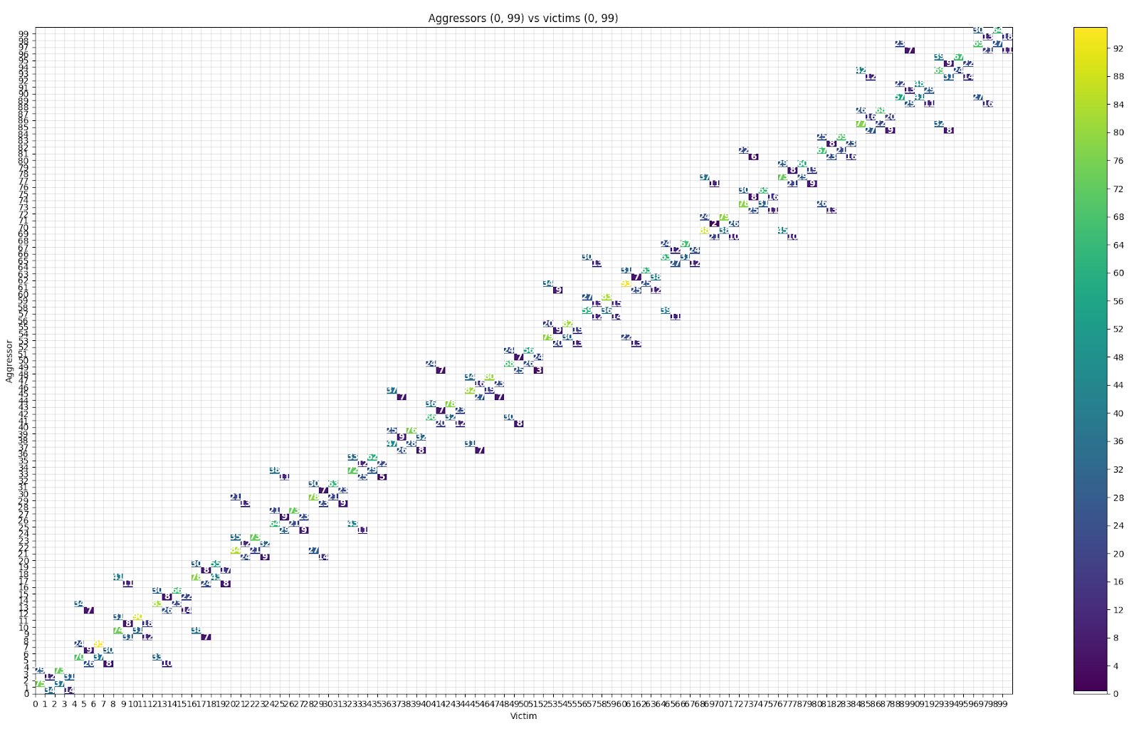
You can also use the logs2dq.py script to visualize bitflips and group them by DQ pad. For details on using the Rowhammer tester and analyzing the results, refer to the project’s documentation.
Security through transparency with Antmicro
Antmicro and Google’s joint work on memory security, as well as common efforts within initiatives such as RISC-V and CHIPS Alliance, aims at providing an open source-based approach across the hardware landscape.
We offer comprehensive engineering services spanning not only DRAM security testing and memory controller development, but also open hardware FPGA-based boards prototyping, ASIC and FPGA verification and testing, and custom data center solutions. If you’re interested in using the Rowhammer testing framework or want to learn how we can help with your next project, don’t hesitate to contact us at contact@antmicro.com.


