Electromagnetic field simulation provides critical data on signal integrity, allowing for iterative design improvements before manufacturing and improved efficiency and reliability when developing dense designs with high-speed interfaces such PCIe Gen 5 and 6, USB 4 or GMSL 3 that we often work with. Antmicro’s popular gerber2ems tool and the complementary wrapper scripts, which we described in more detail in a previous article, help us provide automated and comprehensive testing for complex, multi-layer PCB designs that we develop for our customers.
In this article we describe the recent improvements we introduced to the flow, including adaptive grid generation and differential pair simulation, validated by comparing simulation and Vector Network Analyzer (VNA) measurements of real hardware designs. The related set of tools for simulation and visualization can be either invoked from the command line or automated in CI, and example simulation data for our open source designs can be seen in our Open Hardware Portal.
Faster simulation with adaptive grids
The FTDT (Finite-difference time-domain) method used by the openEMS tool, which we use for processing simulation data, involves dividing the simulation space into a rectilinear grid and solving discrete Maxwell equations for each cell. Discretization requires that the cell is small enough so that the simulated object can be mapped accurately, but at the same time the grid should be as sparse as possible, as each additional cell increases the number of calculations (e.g. making the grid twice as dense increases simulation time more than 8 times). Simulation time is also affected by the grid cell size - the smaller the cell, the smaller the timestep, meaning more timesteps are required. This also results in increased simulation time.
In the original implementation of gerber2ems, we were creating equidistant rectangular grids. With the new adaptive grid approach, we can limit the number of cells, making the grid denser around the simulated geometry and sparser in areas less important for simulation. To do that, first we analyze the input Gerber files and identify the trace of interest’s position and shape in order to find contours of interesting metal (copper) patterns. Then, we place grid lines following the commonly used 1/3 meshing rule, i.e. placing grid lines in a way that a cell created by these lines is 1/3 inside and 2/3 outside the metal element. We also place sparser grid lines where the copper pattern is uniform. As a result, we observed a significant reduction of simulation time, as well as better accuracy.
Differential pair simulation
Simulating differential pairs is crucial when working with high-speed interfaces such as HDMI, USB, PCIe or MIPI CSI-2. Apart from transmission and reflection, we also need to consider trace delay skew between PCB traces which formulate a pair. A skew mismatch can lead to increased EMI susceptibility and distortions in differential signal reception. For that reason some standards specify the maximum values of the intra-pair skew, e.g. for CSI-2 it’s 1 ps. A common engineering practice to reduce skew is to perform length matching of the traces. However, this approach is not ideal, as propagation time depends not only on copper length but also on signal propagation speed, which is dependent on numerous factors, including trace width, nearby metal patterns and frequency.
Being able to simulate trace delay using gerber2ems allows us to verify the correctness of intra-pair length matching and, if necessary, apply corrections, leading to more robust high-speed connections. We also use gerber2ems to generate delay graphs - you can find examples for selected designs on our GitHub.
Improved slice preparation, CI flow, and more
We updated the wrapper scripts to support KiCad 9, which is the most recent version at the time of writing. As described in the previous note, the kicad-si-simulation wrapper is a tool used to specify the Region of Interest (ROI) for the simulation. In particular, it can process the whole PCB (that can be fabricated and used as a part of a device) and extract from it a sub-region with PCB traces that we want to simulate. The wrapping process allows us to apply the OpenEMS solver to real-life PCB designs.
A subset of the input PCB design is called a slice. A slice is defined by adding simulation ports (for applying the stimuli and collecting responses) to the original PCB. Based on the port location, the wrapper tool can automatically extract the PCB trace and surrounding region from the input PCB. The slicing process has now been improved, so that placing the port requires significantly less manual intervention. The slicing algorithm can now also handle typical electronic components (such as TVS diodes) and PCB primitives (vias) that appear along the PCB traces that we want to simulate.
We also developed a tool called ems2paraview which imports simulation results to ParaView, an open source interactive scientific visualization tool. For more details about using ems2paraview, refer to the README.
After the recent updates, the gerber2ems and si-wrapper tools are now able to operate mostly without manual tweaking, which means we can automate the simulation and visualization processes in a CI setup. This becomes especially useful for regression tracking.
We also updated the process of generating animations that employs our KiCad-Blender flow - while it is still partially manual, most of it can now be automated in CI.
Verifying simulation with VNA measurements
Comparing simulation results to VNA measurements allows us to verify the correctness of simulation results. However, measuring with VNA can be tricky, as cables and connectors affect the results, and simple connections with loose wires may provide highly inaccurate results. It can also be difficult to connect to most traces, as they often start and end with fine-pitched components (0.4, 0.5 or 0.8 mm pitch).
For lower band measurements, Antmicro developed an open hardware VNA probe that maintains a controlled 50 Ohm impedance and can be attached even to fine-pitched traces. The probe is compatible with pogo pins and measurement needles that allow us to take measurements by pressing into pads or exposed traces, without the risk of damaging the PCB, and connects to VNA using a standard SMA connector.
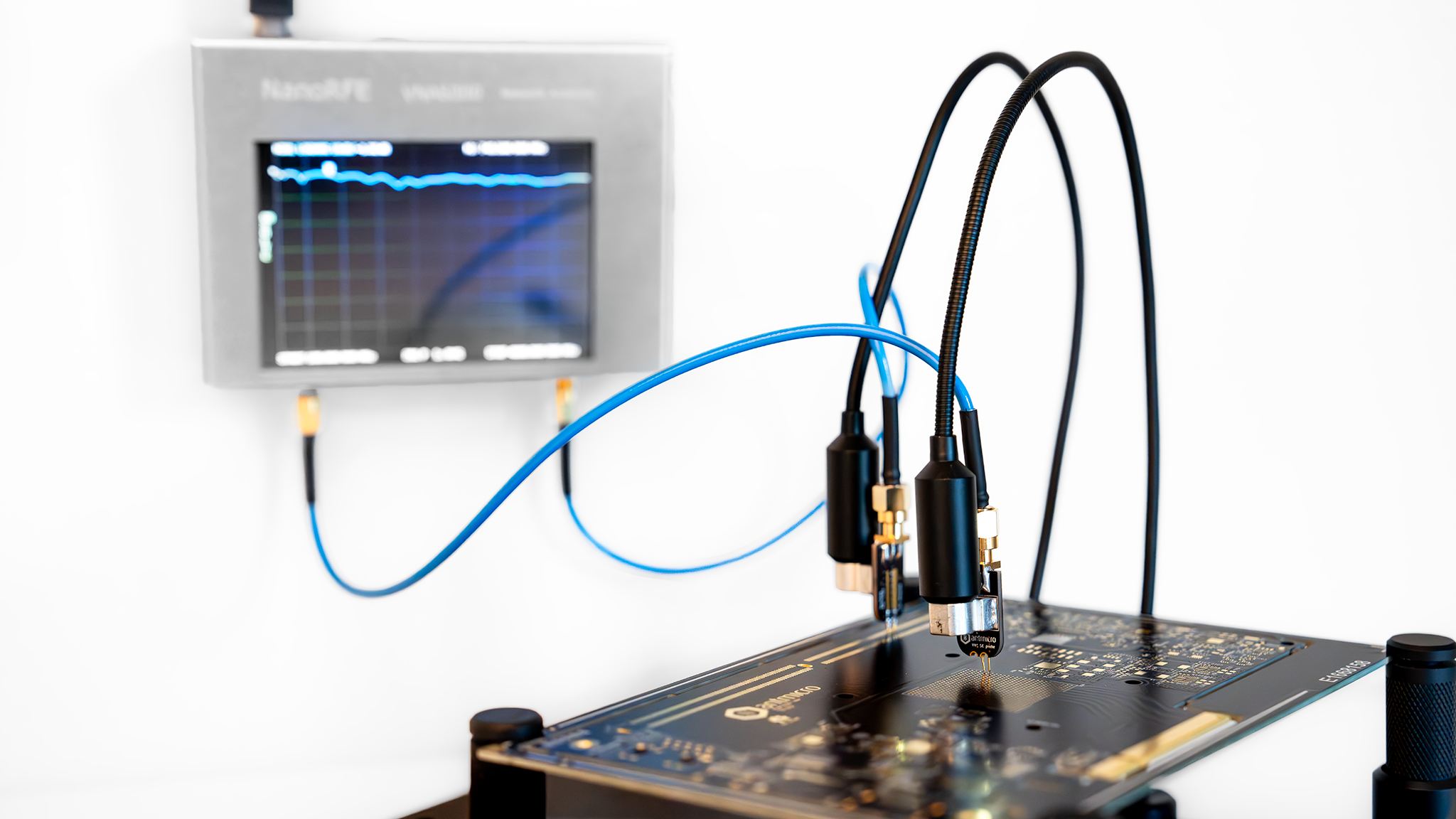
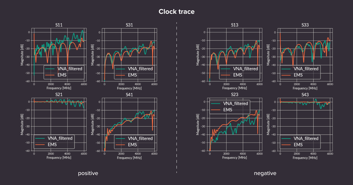
For higher frequencies though, this probe introduces too much distortion and it is recommended to switch to soldering a 50 Ohm coaxial cable directly to the signal pads, even despite the higher risk of damaging the PCB. Using this method we measured a control clock signal on our RDIMM DDR5 Tester and compared the results with gerber2ems simulation.
The resulting S-parameter graphs are presented below for both positive (Sx1) and negative (Sx3) trace of this pair. We can see that the results from EMS and VNA (processed with the Savitzky-Golay filter) match pretty well in both character and order of magnitude. We can see some ripples on S21 and S43 (which correspond to transmission of each line of the differential pair), which are caused by the VNA connection itself slightly altering the characteristics of the measured trace, by adding additional stray capacitance and inductance. With that knowledge, we can confirm that our simulations are able to quite closely predict the behavior of tracks.
CI-driven signal integrity simulation for complex designs
With the improvements described in this article, Antmicro’s signal integrity simulation flow is allowing for easier and more accurate simulation of more complex designs. As we continue to work on the simulation and visualization tools, our goal is to keep the entire process, from design verification to field animation generation, fully automated. We will also continue to introduce more features, e.g. crosstalk analysis.
If you’re interested in building your next device with Antmicro and would like to take advantage of our comprehensive hardware design verification services, including electromagnetic interference analysis and thermal simulation, don’t hesitate to contact as at contact@antmicro.com.

