Antmicro’s typical industrial customer would work with us to create advanced devices based on high-end processing platforms - and the baseboards, adapters and bridges showcased on our Open Hardware Portal are a great starting point for this kind of product development. Typical applications include data capture, edge AI and video processing, therefore we also often design video-related cross-converters, including the SDI to MIPI CSI-2 Converter and the recent GMSL SerDes solution which ultimately get integrated into a single-board final design.
Illustrative of the high-end use cases of our customers, many products derived from our open hardware designs need to be size-constrained, as they target UAVs, drones, industrial robots, autonomous underwater rovers or cube satellites. These applications call for complex, multi-layer PCB designs and are characterized by a high density of component arrangement, where cross-component electromagnetic interferences need to be taken into account. In this note we describe yet another aspect of Antmicro’s open source-based hardware design flow after the recently described simulation-based signal integrity analysis, namely automated EMI scanning of fabricated prototypes.
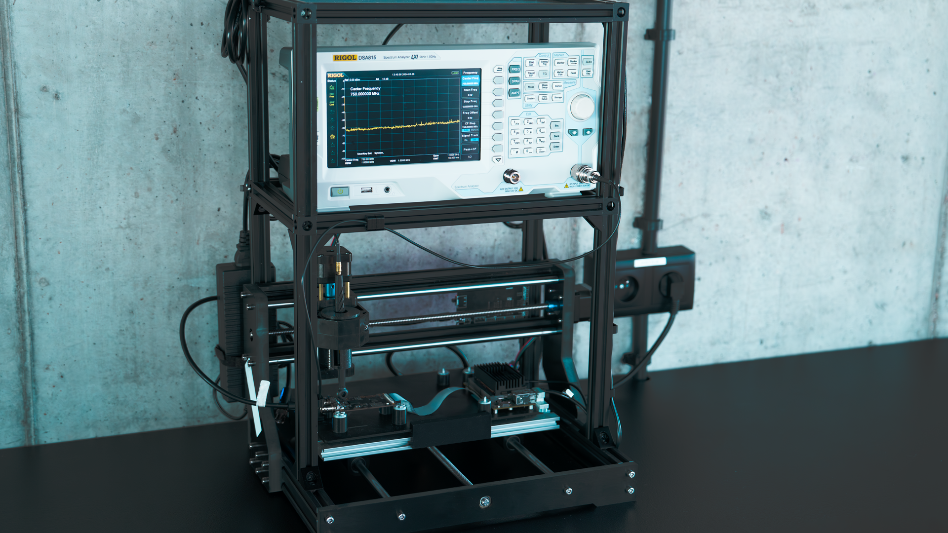
Our EMI measurement solution consists of a spectrum analyzer equipped with near-field probes installed in an axis plotter and orchestrated with Python scripts to enable automatic measurements and result visualization using our Blender-based rendering flow.
Near-field vs far-field testing
Measurements of electromagnetic fields can be divided into near-field and far-field, since the electromagnetic field will behave differently depending on the distance from the emission source. In short: within the near field, the ratio of electric and magnetic wave strength changes over distance and is dependent on the source, while in the far field it remains stable.
Measuring near fields is performed with a probe in order to acquire an image of how the fields spread, but because the electric and magnetic parts of the field act differently in the near field, a different kind of probe must be used for each wave type. Their measuring abilities mostly depend on shape and size of the tip. Electric near-field probes are small antennas which capture electric emissions within small ranges of 3-20mm. A magnetic near-field probe takes the form of a coil, with ranges varying between 20-100mm, so they’re less precise in terms of pinpointing a location of emission source, but more likely to detect it at all.
Legal regulations define limits and tests for far-field measurements, because at this distance the electric and magnetic fields become uniform and more predictable, which makes it easier to standardize and define safe limits of emitted wave’s strength. They are not affected by factors like geometry of the emitting antenna or its immediate surroundings as much as in the near-field. Contrary, near-field testing is rather a debugging tool that helps understand what is happening in the circuit and identify where the emissions are coming from. The near field can be measured locally with dedicated probes and a spectrum analyzer. With handheld tools, it is hard to get comparable results while inspecting a given PCB unit operating in a certain mode, as the probes are very sensitive to position and orientation changes. The magnetic field probe may show completely different results when rotated by 90 degrees, while the electric field probe with a measuring range of a few millimeters may provide varying results because of a slight hand tremble. These issues can be remedied by automating the process.
Automated near-field scanning and integration with Antmicro’s Blender flow
In order to achieve repeatable near-field measurements, for our PoC setup we installed a near-field probe on a 2.5-axis plotter and automated the scanning process. We use a Rigol DSA815 spectrum analyser with Rigol NFP-3 series probes (P2 magnetic field probe and P4 electric field probe), mounted on a generic XY plotting frame with stepper motors and a simple controller that accepts commonly used G-codes. Measurements are taken not further than 1 cm from the board in the Z axis, and with a step smaller than the probes’ ranges.
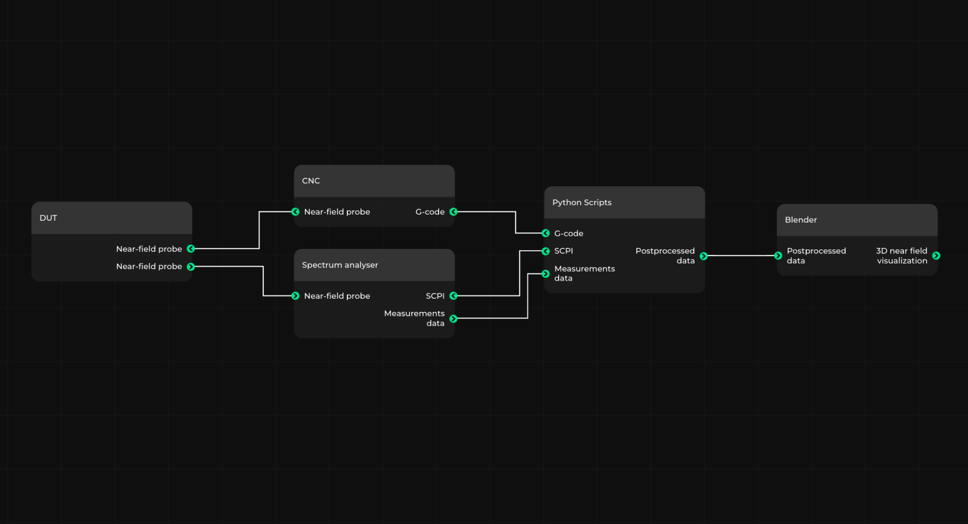
With this setup and a set of Python scripts, you can sample near-field emissions for a mesh of points and compute an emission map of the DUT.
The first script is used for CNC machine control and the spectrum analyzer data capture. It moves the near-field probe above the board, making evenly distributed stops. Communication with the plotter is conducted via serial port and G-code commands. The measurements are captured by the spectrum analyzer controlled via LAN interface and SCPI (Standard Commands for Programmable Instruments) protocol. The script outputs a set of files containing EM field spectral distributions corresponding to a two-dimensional matrix of the measurement points on the DUT board.
The second script is used for data post-processing. This is where the measurement data is aggregated and interpolated to create a heatmap plot representing field distribution across the board in smaller frequency ranges with a step of 50MHz.
Finally, another script is used to visualize the data. It projects the electromagnetic emission heatmaps on a Blender model of the PCB to create a 3D view that shows the radiated field distribution in spatial relation to the board.
For detailed instructions on using the scripts and generating 3D visualizations of the provided sample, refer to the project’s README.
Analyzing the SDI to MIPI CSI-2 bridge
Using our Blender-based visualization flow, we can create detailed renders of the results and even animations showing how the EM field changes at different frequencies. This process is similar to the one we used for SI simulations, however this time we use real-life measurements. The example below shows the results for our open source SDI to MIPI CSI-2 bridge.
This visualization is generated from data collected with a magnetic field probe - P2. Its range is 30mm but the measurements were taken with a 5mm step in both X and Y directions, and a constant position in the Z axis. The probe coil was parallel to the shorter board dimension during the measurement.
The peaks shown in the video above are coming from TP17 that is visibly lying underneath them. This is a testpoint exposing the output of the GS2971A chip’s main clock generator. It was included in the design to make board debugging more convenient, however at the same time it introduces a tiny stub which turns out to be large enough to emit harmonics of its base frequency, 27 MHz. Similar frequencies are visible around TP1. The visualization shows a peak of combined emissions from these sources around 445 MHz.
The approach described above allows us to get reproducible scans of the EM field distribution across the PCB, as well as identify the components and functional blocks - and even PCB traces - that emit energy when stimulated. Since we are using a spectrum analyzer, we can also identify the characteristic frequencies at which field radiation reaches its local peaks. This allows us to identify PCB parts that require special attention during hardware debugging.
With this flow, we can also easily experiment with various PCB shielding techniques that can be applied locally to certain components while preparing for EMI compliance testing for radiated emission in a full-fledged anechoic chamber.
Comprehensive prototyping of size-constrained devices with Antmicro
The solution described in this note enables automated, reproducible near-field EM scanning of a PCB prototype and comprehensive spatial visualization of the field. The flow is very useful for EMI debugging, letting engineers pin-point emission sources and apply countermeasures to ensure electromagnetic compatibility of the designed device.
Antmicro offers a broad range of comprehensive hardware and software development services backed by a suite of constantly developing open source productivity tooling. We help customers in building end-to-end solutions that include hardware design, prototyping, verification, testing and productization. On top of that we develop customized Board Support Packages tailored for particular use cases with remote management and Over-The-Air update capabilities. Customers also benefit from our CI-driven, reproducible hardware rendering flow allowing them to visualize the device long before it becomes a physical prototype.
If you’re interested in designing a size-constrained device with us or would like to learn more about the unified and reproducible flow for EMI testing of PCBs that we design, reach out to us at contact@antmicro.com.


