Antmicro has created a broad portfolio of open source hardware designs that constitute a perfect entry point for product development, as showcased on our Open Hardware Portal. Since a lot of our projects focus on complex applications such as video processing or high-speed connectivity, the vast majority of our PCBs require impedance-controlled nets that must be designed following strict criteria to ensure signal integrity. This is especially important to the performance of high-speed digital interfaces, such as MIPI CSI-2, DDR or PCIe.
As described on our blog some time ago, basing on the openEMS library, Antmicro created a tool called gerber2ems that converts PCB production files, generated with e.g. KiCad, into PNGs which can then in turn be further processed and used for simulation with openEMS.
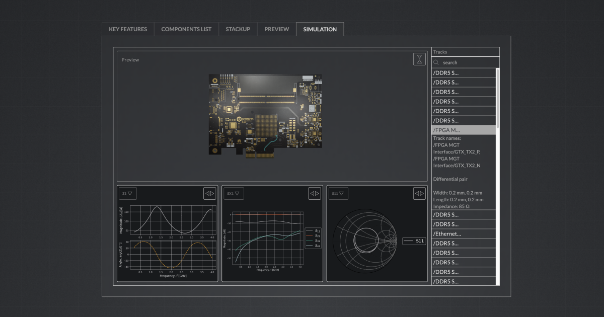
Signal integrity simulation provides invaluable aid in prototyping complex designs, such as DDR5 memories, high speed FPGAs and SoCs, quicker and more reliably. To further improve this flow, we’ve developed wrapper scripts that generate input data for SI simulation, which we’ll describe in this article along with an example simulation for our open hardware SO-DIMM (LP)DDR5 Tester. To showcase this data for our designs, we also introduced it to our Open Hardware Portal in a dedicated Simulation tab for selected boards, with more examples coming soon.
Signal integrity simulation flow
To prepare input data for simulations, first we need to select critical traces to be simulated. Due to the complexity of the simulation process, each trace or differential pair needs to be considered separately. Simulation ports need to be placed at the beginning and the end of the simulated trace and other copper fields need to be reduced, cleaned and terminated (assigned an impedance at the ends). Before, we performed these actions manually - now we are adding an automated solution to aid the process, namely a set of scripts for generating the simulation cases and organizing the output.
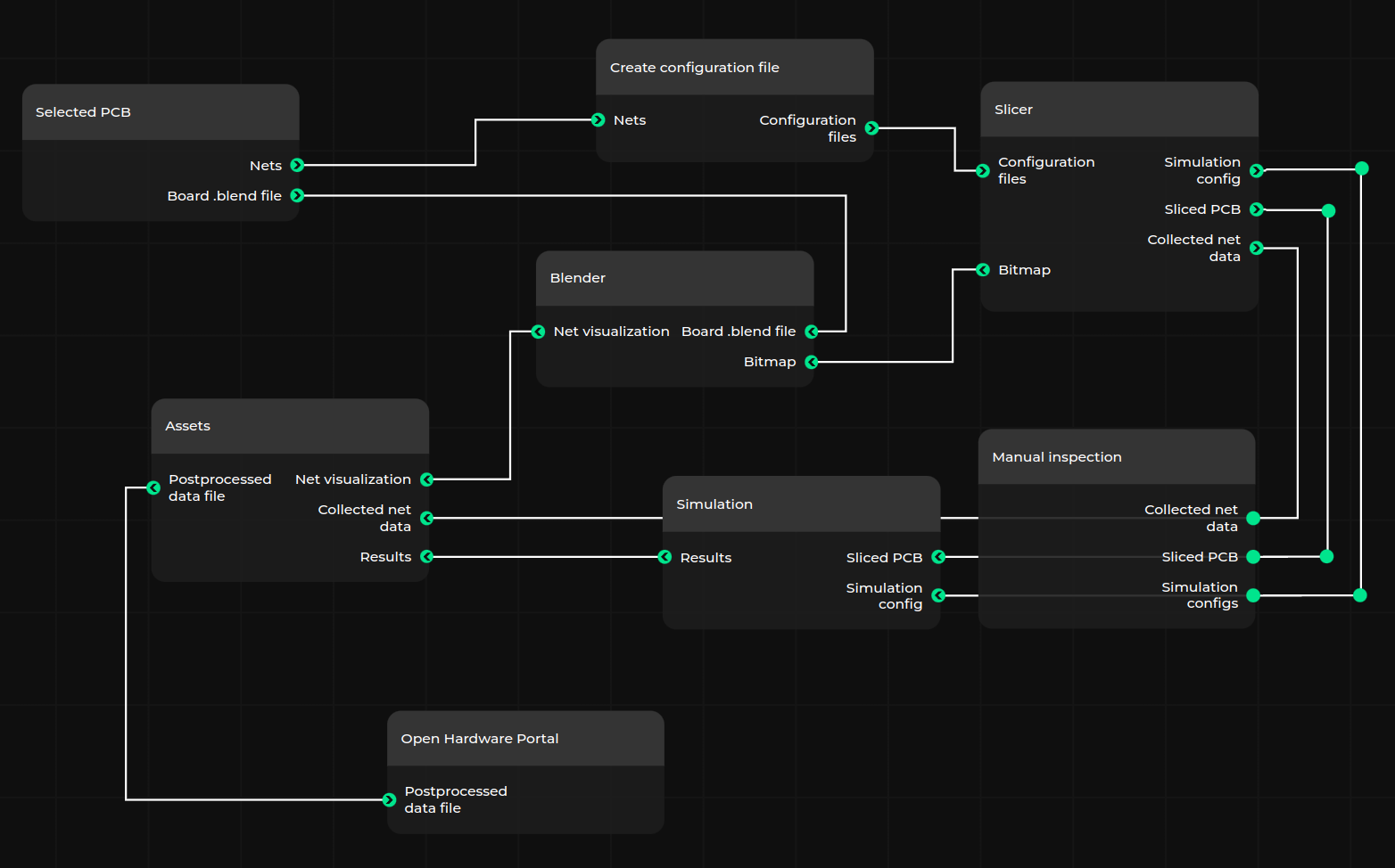
The current flow for performing signal integrity simulation, visualized in the diagram below, consists of the following steps:
- Selecting signal nets to be simulated
- Creating simulation cases - PCB slices and simulation configuration files
- Manual data adjustment - user can alter the simulation setting or port placement
- Exporting PCB slices to a 3D mesh of conductive/dielectric primitives with
gerber2ems - Simulation with OpenEMS
- Generating visualizations of the simulation results
- Presenting the board simulation summary on Open Hardware Portal
Creating a PCB slice
Our OSHW boards are designed in KiCad which provides great flexibility including custom scripts and plugins. The KiCad Pcbnew Python API provides PCB modification capabilities with Python scripting. Based on that, we created a Python package that prepares input data for our signal integrity analysis workflow.
si-wrapper slice creates simulation cases - board slices of the analyzed PCB, which are the main input to the gerber2ems script. As the slice covers a particular net, its minimal size is determined by the span of the net. The script’s config defines the size of a margin added to the minimal dimension, and criteria of inclusion of neighboring nets - parts of signal traces next to the analyzed net/pair, which can influence signal propagation and should be included in the simulation.
A slice prepared for simulation contains the designated net (or a pair of nets in case of a differential pair), neighboring nets and all vias and planes present in the area. Passive elements like 0 Ω resistors and significantly large capacitors are replaced with a short - a trace connecting pads of their footprints. This approximation is valid for our frequencies of interest and allows us to circumvent limitations of the OpenEMS simulator. The neighboring nets are terminated with their nominal impedance. In case of power nets and low speed interfaces, a 0 Ω termination is assumed.
The final operation in preparing the PCB slice is the placement of the Simulation Ports on the analyzed net, as well as the neighboring nets.
Simulation Ports
A Simulation Port represents a signal source and sink in the simulation. A single net simulation requires two Simulation Ports, while a differential pair should be marked with four. Analogically, the neighboring nets require placement of the Simulation Ports, representing their termination impedance.
The si-wrapper slice script automatically determines the correct positions of the ports and pinpoints them with markers, implemented as a virtual KiCad footprint. The ports are placed at the beginning and the end of a particular net. The script searches for KiCad components connected to the net, and marks the end of the net’s trace section closest to the center of the terminating component pad. The port orientation is determined based on the pad orientation. The simulation software limits the port orientation to one of the four major directions on the plane. Every Simulation Port has an assigned number which can be also found inside the simulation configuration.
If the si-wrapper slice script fails to identify the correct number of ports - which can happen, for example, if the trace fails to follow the two-point configuration, which is recommended for a high-speed routing - it prompts the user to adjust the port placement. This can be achieved by editing the PCB slice with KiCad, and running si-wrapper renumerate.
Simulation configuration
The simulation configuration file and net information file are generated along with the slice. The simulation configuration file contains all crucial simulation parameters that can be adjusted, but the default settings work in the majority of cases. The configurable parameters are described in the gerber2ems README. The net information file consists of the designated net name, width, length, impedance, single/differential net flag, and temporary links to the results.
Simulation results for the SO-DIMM (LP)DDR5 tester
Using the flow described above, we performed a simulation for our open hardware SO-DIMM (LP)DDR5 tester. This board features a DDR5 interface (or, in an alternative configuration, LPDDR5), which, due to high clock speeds, is particularly sensitive to signal integrity issues. Simulation of the memory interface’s clock, address and data traces provides a valuable tool for verification and quality assurance of the design.
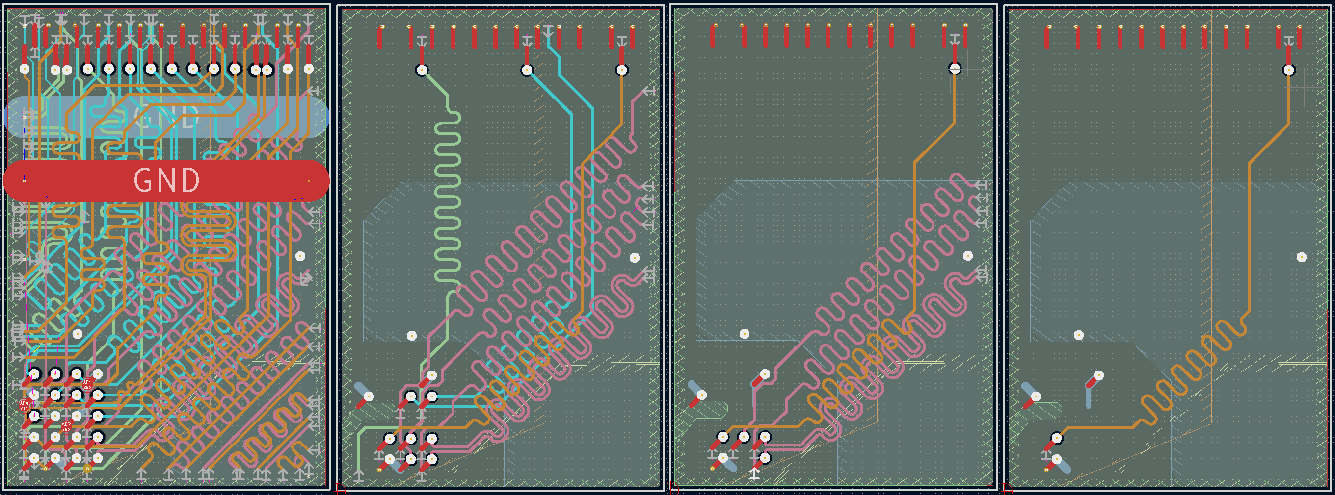
Below, we show examples of the PCB slice preparation for the /DDR5 SODIMM/B.DQ12 net with different settings for neighboring. The first one has no reduced layout, the second has the neighboring net threshold set to 2 neighboring points, the third to 10 neighboring points and the fourth to 50 neighboring points. The neighboring net distance offset is set to 0.3 mm for each case. This helps get rid of the tracks that have little impact on signal integrity of the analyzed net and makes the simulation case for the OpenEMS significantly less complex. We generate simulation cases for the whole PCB by picking nets from the “controlled impedance” class defined in the KiCad project. The selection is performed by the si-wrapper settings script. Subsequently, the selected nets are processed with si-wrapper slice to produce the simulation cases.
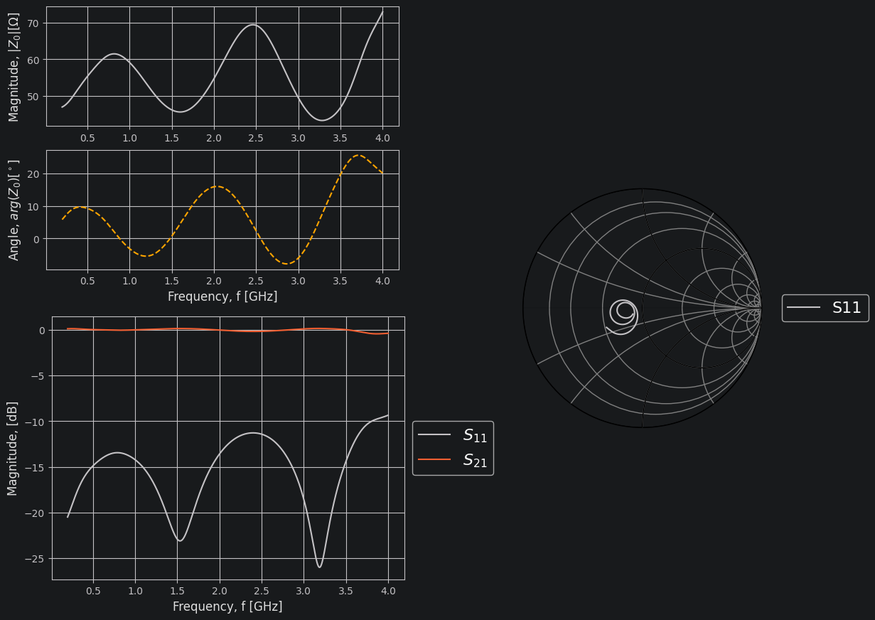
The diagrams below show the simulation results. On the left, there are charts of the trace’s impedance observed from the source port and the trace’s S-parameters in relation to signal frequency. S-parameters are a representation of a response of an N-port network to signals incident to any of the ports. The Smith chart on the right shows a plot of a complex reflection overlaid with an impedance and admittance grid referenced to characteristic impedance of the trace. Based on these charts, we can draw a conclusion that the net was designed correctly.
The animation below shows the simulated signal on a 3D render of the SO-DIMM (LP)DDR5 Tester, created with our KiCad-Blender flow:
Developing complex designs with a comprehensive open source toolkit
Antmicro offers end-to-end hardware design services based on our open source toolkits and workflows, including interactive system diagrams, automatically generated 3D renders and a vast component database, for an iterative and software-driven design process. To ensure automated and comprehensive testing for complex, multi-layer PCB designs before they’re manufactured, our workflow includes not only signal integrity analysis with S-parameter, impedance, Smith etc. charts and eye diagrams, but also electromagnetic field scanning which is crucial for size-constrained devices.
If you want to learn more about how Antmicro’s engineering services can help you reliably design, test and build complete devices using open source tools, don’t hesitate to contact us at contact@antmicro.com.